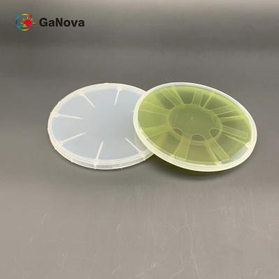
Κρυσταλλική γκοφρέτα SIC
(42)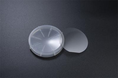
2 ιντσών συσκευή ισχύος υψηλής κινητικότητας ηλεκτρονίων τρανζίστορ επιταξιακή πλάκα
Τιμή: Negotiable
MOQ: 5
Ωρα παράδοσης: Negotiable
Μάρκα: Ganova
Υψηλό Φως:sic epitaxial wafer 2 Inch, Power Device sic epitaxial wafer, High Electron Mobility Transistor Epitaxial Wafer
Introduction to GaN on Silicon HEMT Epi wafer Silicon based gallium nitride HEMT epitaxial wafer is a high electron mobility transistor (HEMT) epitaxial wafer based on gallium nitride (GaN) material. Its structure mainly includes AlGaN barrier layer, GaN channel layer, AlN buffer layer, and silicon ... Δείτε περισσότερα
➤ Επίσκεψη Δικτυακός τόπος
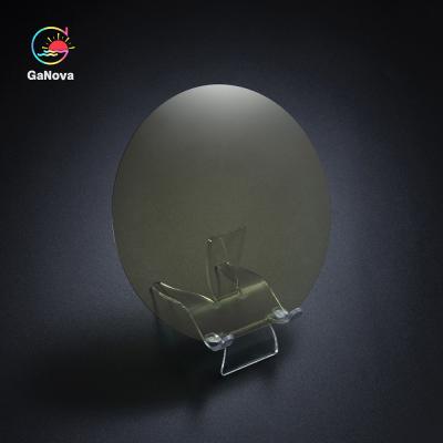
2 ίντσες GaN σε Silicon HEMT Epi σφαιρίδιο για συσκευή ισχύος
Τιμή: Negotiable
MOQ: 5
Ωρα παράδοσης: Negotiable
Μάρκα: Ganova
Υψηλό Φως:GaN On Silicon HEMT Epi Wafer, 2 Inch Epi Wafer, Power Device Epi Wafer
Introduction to GaN on Silicon HEMT Epi wafer Silicon based gallium nitride HEMT epitaxial wafer is a high electron mobility transistor (HEMT) epitaxial wafer based on gallium nitride (GaN) material. Its structure mainly includes AlGaN barrier layer, GaN channel layer, AlN buffer layer, and silicon ... Δείτε περισσότερα
➤ Επίσκεψη Δικτυακός τόπος
Αντικατάστατο AlGaN 4 ίντσες GaN στο Silicon HEMT Epi wafer νιτρίδιο γαλλίου GaN-on-Si
Τιμή: Negotiable
MOQ: 5
Ωρα παράδοσης: Negotiable
Μάρκα: Ganova
Υψηλό Φως:4 inch sic epitaxial wafer, 4 inch sic epi wafer, 4 inch sic epi wafers
Introduction to GaN on Silicon HEMT Epi wafer Silicon based gallium nitride HEMT epitaxial wafer is a high electron mobility transistor (HEMT) epitaxial wafer based on gallium nitride (GaN) material. Its structure mainly includes AlGaN barrier layer, GaN channel layer, AlN buffer layer, and silicon ... Δείτε περισσότερα
➤ Επίσκεψη Δικτυακός τόπος
6 ίντσες GaN σε πυρίτιο HEMT Epi Wafer Power Device Νιτρικό Γαλλίου GaN σε Si
Τιμή: Negotiable
MOQ: 5
Ωρα παράδοσης: Negotiable
Μάρκα: Ganova
Υψηλό Φως:6 Inch sic epitaxial wafer, 6 Inch sic epi wafer, 6 Inch sic epi wafers
Introduction to GaN on Silicon HEMT Epi wafer Silicon based gallium nitride HEMT epitaxial wafer is a high electron mobility transistor (HEMT) epitaxial wafer based on gallium nitride (GaN) material. Its structure mainly includes AlGaN barrier layer, GaN channel layer, AlN buffer layer, and silicon ... Δείτε περισσότερα
➤ Επίσκεψη Δικτυακός τόπος
GaN βιόλετ λέιζερ σε πυρίτιο 2 ίντσες GaN σε πυρίτιο HEMT Epi wafer UV LD Epi wafer
Τιμή: Negotiable
MOQ: 5
Ωρα παράδοσης: Negotiable
Μάρκα: Ganova
Υψηλό Φως:2 inch sic epitaxial wafer, 2 inch sic epi wafer, 2 inch sic epi wafers
Introduction to GaN on Silicon HEMT Epi wafer Silicon based gallium nitride HEMT epitaxial wafer is a high electron mobility transistor (HEMT) epitaxial wafer based on gallium nitride (GaN) material. Its structure mainly includes AlGaN barrier layer, GaN channel layer, AlN buffer layer, and silicon ... Δείτε περισσότερα
➤ Επίσκεψη Δικτυακός τόπος
2 ίντσες GaN στο Σιλικόνιο Μπλε LD Epi Wafer GaN μπλε λέιζερ στο Σιλικόνιο
Τιμή: Negotiable
MOQ: 5
Ωρα παράδοσης: Negotiable
Μάρκα: Ganova
Υψηλό Φως:2 inch sic epitaxial wafer, 2 inch sic epi wafer, 2 inch sic epi wafers
Introduction to GaN on Silicon HEMT Epi wafer Silicon based gallium nitride HEMT epitaxial wafer is a high electron mobility transistor (HEMT) epitaxial wafer based on gallium nitride (GaN) material. Its structure mainly includes AlGaN barrier layer, GaN channel layer, AlN buffer layer, and silicon ... Δείτε περισσότερα
➤ Επίσκεψη Δικτυακός τόπος
Μπλε LED GaN σε κυψέλη πυριτίου Μπλε λέιζερ GaN επιταξιακή κυψέλη
Τιμή: Negotiable
MOQ: 5
Ωρα παράδοσης: Negotiable
Μάρκα: Ganova
Υψηλό Φως:Silicon Based Gallium Nitride Epitaxial Wafer, HEMT epitaxial wafer, 4 inch sic epitaxial wafer
Introduction to GaN on Silicon HEMT Epi wafer Silicon based gallium nitride HEMT epitaxial wafer is a high electron mobility transistor (HEMT) epitaxial wafer based on gallium nitride (GaN) material. Its structure mainly includes AlGaN barrier layer, GaN channel layer, AlN buffer layer, and silicon ... Δείτε περισσότερα
➤ Επίσκεψη Δικτυακός τόπος
2 ιντσών GaN στο Silicon Green LED Epi Wafer Νιτρικό Γαλλίου στο Silicon
Τιμή: Negotiable
MOQ: 5
Ωρα παράδοσης: Negotiable
Μάρκα: Ganova
Υψηλό Φως:2 inch sic epitaxial wafer, 2 inch sic epi wafer, 2 inch sic epi wafers
Introduction to GaN on Silicon Green LED Epi wafer GaN on Silicon Green LED Epi wafer are semiconductor structures formed on silicon substrate materials through epitaxial growth technology for manufacturing green light-emitting diodes (LEDs). It is a key intermediate material in the manufacturing of... Δείτε περισσότερα
➤ Επίσκεψη Δικτυακός τόπος

4 ιντσών GaN σε Silicon Green LED Epi Wafer SiC επιταξιακές πλακέτες
Τιμή: 1000
MOQ: 5
Ωρα παράδοσης: Negotiable
Μάρκα: Ganova
Υψηλό Φως:4 inch sic epitaxial wafer, 4 inch sic epi wafer, 4 inch sic epi wafers
Introduction to GaN on Silicon Green LED Epi wafer GaN on Silicon Green LED Epi wafer are semiconductor structures formed on silicon substrate materials through epitaxial growth technology for manufacturing green light-emitting diodes (LEDs). It is a key intermediate material in the manufacturing of... Δείτε περισσότερα
➤ Επίσκεψη Δικτυακός τόπος

4 ιντσών UGaN σε νιτρίδιο γαλλίου χωρίς ντόπινγκ σε κυψέλη πυριτίου
Τιμή: 1000
MOQ: 5
Ωρα παράδοσης: Negotiable
Μάρκα: Ganova
Υψηλό Φως:4 inch sic epitaxial wafer, 4 inch sic epi wafer, 4 inch sic epi wafers
Introduction to GaN on Silicon Green LED Epi wafer GaN on Silicon Green LED Epi wafer are semiconductor structures formed on silicon substrate materials through epitaxial growth technology for manufacturing green light-emitting diodes (LEDs). It is a key intermediate material in the manufacturing of... Δείτε περισσότερα
➤ Επίσκεψη Δικτυακός τόπος

κρυσταλλική γκοφρέτα 150.0mm +0mm/-0.2mm SIC κανένα δευτεροβάθμιο επίπεδο 3mm
Τιμή: Negotiable
MOQ: Negotiable
Ωρα παράδοσης: 3-4 week days
Μάρκα: GaNova
Υψηλό Φως:150.0 mm SiC Epitaxial Wafer, silicon carbide wafer 3mm, SiC Epitaxial Wafer No Secondary Flat
JDCD03-001-003 Overview SiC boules (crystals) are grown, machined into ingots, and then sliced into substrates, which are subsequently polished. A thin SiC epitaxial layer is then grown on top of this substrate to create an epi-wafer. Today, the semiconductor industry is expanding at a rapid rate, w... Δείτε περισσότερα
➤ Επίσκεψη Δικτυακός τόπος
47,5 χιλ. ± 1,5 κρυσταλλική γκοφρέτα 150,0 χιλ. +0mm/-0.2mm παράλληλο to<11-20>±1° χιλ. SIC
Τιμή: Negotiable
MOQ: Negotiable
Ωρα παράδοσης: 3-4 week days
Μάρκα: GaNova
Υψηλό Φως:446mm SiC Epitaxial Wafer, 4 H epitaxial silicon wafer, UKAS SiC Epitaxial Wafer
47.5 mm ± 1.5 mm SiC Epitaxial Wafer 150.0 mm +0mm/-0.2mm Parallel to±1° JDCD03-001-003 Overview Currently, there are two main types of SiC wafers. The first type is the polished wafer, which is a single silicon carbide disc. It is made of high-purity SiC crystals, and can be 100mm or 150mm in diame... Δείτε περισσότερα
➤ Επίσκεψη Δικτυακός τόπος

4H κρυσταλλική γκοφρέτα ≤0.2 το /cm2 0.015Ω SIC•εκατ.-0.025Ω•εκατ. 150,0 χιλ. +0mm/-0.2mm
Τιμή: Negotiable
MOQ: Negotiable
Ωρα παράδοσης: 3-4 week days
Μάρκα: GaNova
Υψηλό Φως:4H SiC Epitaxial Wafer, silicon carbide wafer ISO9001, SiC Epitaxial Wafer 0.2 /Cm2
4H SiC Epitaxial Wafer ≤0.2 /Cm2 0.015Ω•Cm—0.025Ω•Cm 150.0 mm +0mm/-0.2mm JDCD03-001-004 Overview The 200-mm wafers can be used for a variety of applications. These wafers are 50% thinner than the standard silicon wafer, so the 200-mm diameter can be used for more SiC devices. The 200-mm size is muc... Δείτε περισσότερα
➤ Επίσκεψη Δικτυακός τόπος

4H κρυσταλλική γκοφρέτα 0.015Ω SIC•εκατ.-0.025Ω•Εκατ. ≤4000/cm ² 150,0 χιλ. +0mm/-0.2mm
Τιμή: Negotiable
MOQ: Negotiable
Ωρα παράδοσης: 3-4 week days
Μάρκα: GaNova
Υψηλό Φως:4H SiC Epitaxial Wafer, silicon epi wafer 0.025Ω•Cm, SiC Epitaxial Wafer 0.015Ω•Cm
4H SiC Epitaxial Wafer 0.015Ω•cm—0.025Ω•cm ≤4000/cm2 150.0 mm +0mm/-0.2mm JDCD03-001-003 Overview The next type is beta silicon carbide. Beta SiC is produced at temperatures higher than 1700 degrees Celsius. Alpha carbide is the most common, and has a hexagonal crystal structure similar to Wurtzite.... Δείτε περισσότερα
➤ Επίσκεψη Δικτυακός τόπος

Υπόστρωμα SiC επιπέδου 2 ιντσών για ηλεκτρικές συσκευές και συσκευές μικροκυμάτων
Τιμή: Negotiable
MOQ: Negotiable
Ωρα παράδοσης: 3-4 week days
Μάρκα: GaNova
Υψηλό Φως:P Level SiC Substrate, Microwave Devices silicon carbide substrate, 2 Inch SiC Substrate
P-Level 4H-N/SI260um±25um 2-Inch SiC Substrate For Power Devices And Microwave Devices JDCD03-001-001 2-inch SiC substrate P-level 4H-N/SI260μm±25μm for power devices and microwave devices Overview Key features Optimizes targeted performance and total cost of ownership for next generation power elec... Δείτε περισσότερα
➤ Επίσκεψη Δικτυακός τόπος

Υπόστρωμα SiC 2 ιντσών 350μm για απαιτητικά ηλεκτρονικά ισχύος
Τιμή: Negotiable
MOQ: Negotiable
Ωρα παράδοσης: 3-4 week days
Μάρκα: GaNova
Υψηλό Φως:2 Inch SiC Substrate, Demanding Power Electronics 2 inch wafer, SiC Substrate 350um
P-Level 2-Inch SiC Substrate 4H-N/SI260μm±25μm For Demanding Power Electronics JDCD03-001-001 2-inch SiC substrate P-level 4H-N/SI260μm±25μm for power devices and microwave devices Overview High crystal quality for demanding power electronics As transportation, energy and industrial markets evolve, ... Δείτε περισσότερα
➤ Επίσκεψη Δικτυακός τόπος
0.015Ω•εκατ.-0.025Ω•SIC κρυσταλλικού γκοφρετών εκατ. Si-προσώπου CMP γ-προσώπου οπτικού πολωνικού
Τιμή: Negotiable
MOQ: Negotiable
Ωρα παράδοσης: 3-4 week days
Μάρκα: GaNova
Υψηλό Φως:SiC Epitaxial Wafer C-Face, Optical Polish sic wafer, Si-Face CMP Sic Epitaxial Wafer
0.015Ω•cm—0.025Ω•cm SiC Epitaxial Wafer C-Face:Optical Polish,Si-Face CMP Overview A SiC wafer is a semiconductor material made of silicon. A silicon carbide wafer is a crystalline material that is made by etching the crystal. It is typically thin enough to be used for power semiconductor devices. T... Δείτε περισσότερα
➤ Επίσκεψη Δικτυακός τόπος
Επίπεδο P υποστρώματος καρβιδίου πυριτίου 260μm για ηλεκτρικές συσκευές και συσκευές μικροκυμάτων
Τιμή: Negotiable
MOQ: Negotiable
Ωρα παράδοσης: 3-4 week days
Μάρκα: GaNova
Υψηλό Φως:260um silicon carbide substrate, Power Devices Epitaxial Wafer, silicon carbide substrate P Level
4H-N/SI260μm±25μm 2-Inch SiC Substrate P-Level For Power Devices And Microwave Devices JDCD03-001-001 2-inch SiC substrate P-level 4H-N/SI260μm±25μm for power devices and microwave devices Overview We contribute to the SiC success story by developing and manufacturing market-leading quality SiC subs... Δείτε περισσότερα
➤ Επίσκεψη Δικτυακός τόπος

Πολυτύπος Κανένα Επιτρεπτό SiC Επιταξιακή γκοφρέτα P-MOS P-SBD D Κατηγορία
Τιμή: Negotiable
MOQ: Negotiable
Ωρα παράδοσης: 3-4 week days
Μάρκα: GaNova
Υψηλό Φως:SiC Epitaxial Wafer P-MOS, D Grade silicon epi wafer, SiC Epitaxial Wafer P-SBD
JDCD03-001-004 Sic Epitaxial Wafer P-MOS P-SBD D Grade Polytype None Permitted JDCD03-001-004 Overview A SiC wafer is a semiconductor material that has excellent electrical and thermal properties. It is a high-performance semiconductor that is ideal for a wide variety of applications. In addition to... Δείτε περισσότερα
➤ Επίσκεψη Δικτυακός τόπος