
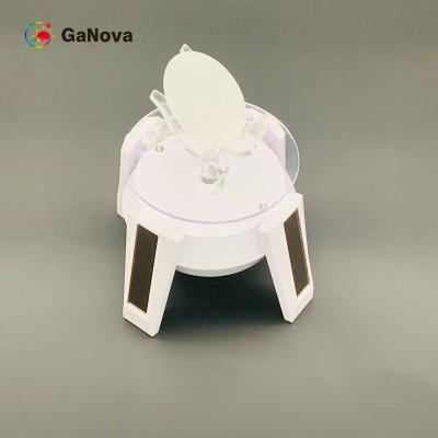
Σύστημα αναψύξης RTP-SA-8 για ταχεία θερμική επεξεργασία
Τιμή: Negotiable
MOQ: Negotiable
Ωρα παράδοσης: 3 month
Μάρκα: Ganova
Υψηλό Φως:Boost Production Rapid Thermal Processing, Rapid Thermal Processing Annealing System
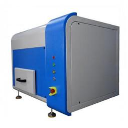
1.Basic configuration of equipment system 1.1outline The Rapid Thermal Processing is a vertical semi-automatic 8-inch wafer rapid annealing furnace, which uses two layers of infrared halogen lamps as heat sources for heating. The internal quartz cavity is insulated and insulated, and the outer shell... Δείτε περισσότερα
➤ Επίσκεψη Δικτυακός τόπος
το γρήγορο θερμικό ανοπτώντας σύστημα 150mm με τρία σύνολα επεξεργάζεται τα αέρια
Τιμή: Negotiable
MOQ: 1
Ωρα παράδοσης: 8-10week days
Μάρκα: GaNova
Υψηλό Φως:150mm Rapid Thermal Annealing System, desktop rapid thermal processing equipment, Wafer Rapid Thermal Annealing System
RTP-150RL Rapid Thermal Annealing System with Three Sets Process Gases RTP-150RL: Is in the protection atmosphere of the desktop manual rapid annealing system, with infrared visible light heating single piece Wafer or sample, short process time, high temperature control precision, suitable for 2-6 i... Δείτε περισσότερα
➤ Επίσκεψη Δικτυακός τόπος

JDCD05-001-003 10*10mm2*0.3mm ηλεκτρονικό διαμάντι ενιαίου κρυστάλλου βαθμού, Ν Content<100ppb, θερμική αγωγιμότητα XRD<0.015º
Τιμή: Negotiable
MOQ: Negotiable
Ωρα παράδοσης: 3-4 week days
Μάρκα: GaNova
Υψηλό Φως:Electronic Grade Single Crystal Diamond, 10*10mm2*0.3mm Single Crystal Diamond
διαμάντι ενιαίου κρυστάλλου βαθμού 10*10mm2*0.3mm ηλεκτρονικό, περιεχόμενο Ν<100ppb>
ΕπισκόπησηΟι μονοκρυσταλλικές γκοφρέτες διαμαντιών επιτρέπουν τις κρίσιμες προόδους και στην τεχνολογία δύναμης RF που χρησιμοποιείται για τις επικοινωνίες και τους δορυφόρους 5G όπως και στην ηλεκτρονικ... Δείτε περισσότερα
➤ Επίσκεψη Δικτυακός τόπος
JDCD05-001-006 10*10mm2*0.5mm ηλεκτρονικό διαμάντι ενιαίου κρυστάλλου βαθμού, Ν Content<100ppb, θερμική αγωγιμότητα XRD<0.015º
Τιμή: Negotiable
MOQ: Negotiable
Ωρα παράδοσης: 3-4 week days
Μάρκα: GaNova
Υψηλό Φως:10*10mm2*0.5mm Single Crystal Diamond
JDCD05-001-006 10*10mm2*0.5mm ηλεκτρονικό διαμάντι ενιαίου κρυστάλλου βαθμού, περιεχόμενο Ν<100ppb>
Επισκόπηση
CVD το διαμάντι έχει αναγνωριστεί από καιρό ως τελευταίο υλικό σε μια ευρεία ποικιλία των εφαρμογών λόγω των ακραίων ιδιοτήτων του.
Για CVD διαμαντιών τα παιχνίδια ατομικού... Δείτε περισσότερα
➤ Επίσκεψη Δικτυακός τόπος
4 ιντσών P-Type Mg-Doped GaN On Sapphire Wafer SSP Resistivity~10Ω Cm Επιταξιακή γκοφρέτα λέιζερ LED PIN
Τιμή: Negotiable
MOQ: Negotiable
Ωρα παράδοσης: 3-4 week days
Μάρκα: GaNova
Υψηλό Φως:LED Laser PIN Epitaxial Wafer
4 ιντσών P-type Mg-doped GaN σε γκοφρέτα ζαφείρι SSP αντίσταση~10Ω cm LED, λέιζερ, επιταξιακή γκοφρέτα PIN
Οι ηλεκτρικές ιδιότητες του GaN με πρόσμιξη Mg τύπου p διερευνώνται μέσω μετρήσεων φαινομένου Hall μεταβλητής θερμοκρασίας.Δείγματα με ένα εύρος συγκεντρώσεων ντόπινγκ Mg παρασκευάστηκαν με... Δείτε περισσότερα
➤ Επίσκεψη Δικτυακός τόπος
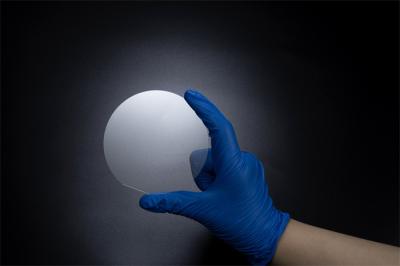
JDCD05-001-005 5*5mm2*0,5mm Electronic Grade Single Crystal Diamond,N Content
Τιμή: Negotiable
MOQ: Negotiable
Ωρα παράδοσης: 3-4 week days
Μάρκα: GaNova
Υψηλό Φως:XRD<0.015º Single Crystal Diamond
JDCD05-001-005 5*5mm2*0,5mm ηλεκτρονικής ποιότητας διαμάντι μονού κρυστάλλου, περιεχόμενο N<100ppb, XRD<0,015º Θερμική αγωγιμότητα 1000-2200 για ψύκτρα
ΣΦΑΙΡΙΚΗ ΕΙΚΟΝΑ
Η υψηλή θερμική αγωγιμότητα του διαμαντιού το έχει κάνει χρήσιμο σε εφαρμογές διαχείρισης θερμότητας.Η ευρεία γκάμα οπτικ... Δείτε περισσότερα
➤ Επίσκεψη Δικτυακός τόπος
Ναρκωμένη Φε ειδική αντίσταση υποστρωμάτων GaN > 10 ⁶ Ω·Συσκευές εκατ. RF
Τιμή: Negotiable
MOQ: Negotiable
Ωρα παράδοσης: 3-4 week days
Μάρκα: GaNova
Υψηλό Φως:ISO GaN Substrates, gan semiconductor wafer, Fe Doped GaN Substrates
2inch C-face Fe-doped SI-type free-standing GaN single crystal substrate Resistivity > 106 Ω·cm RF devices The achieved breakdown voltage of the Fe-doped GaN epitaxial layer can be as high as 2457 V, which is attributed to the Fe-doped GaN epitaxial layer with higher resistance, which can sustain... Δείτε περισσότερα
➤ Επίσκεψη Δικτυακός τόπος
625um σε 675um κρυσταλλική γκοφρέτα GaN 4 μπλε οδηγήσεων ίντσας στον επίπεδο σάπφειρο SSP σαπφείρου
Τιμή: Negotiable
MOQ: Negotiable
Ωρα παράδοσης: 3-4 week days
Μάρκα: GaNova
Υψηλό Φως:625um GaN Epitaxial Wafer, SSP gan on sapphire wafers, 675um GaN Epitaxial Wafer
Substrate Thickness 650 ± 25 μm 4 Inch Blue LED GaN Epitaxial Wafer On Sapphire SSP Flat Sapphire 4 inch Blue LED GaN epitaxial wafer on sapphire SSP For example, GaN is the substrate which makes violet (405 nm) laser diodes possible, without use of nonlinear optical frequency-doubling. Its sensitiv... Δείτε περισσότερα
➤ Επίσκεψη Δικτυακός τόπος
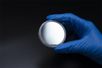
Γ-επίπεδη γκοφρέτα υποστρωμάτων σαπφείρου JDCD08-001-006 6inch
Τιμή: Negotiable
MOQ: Negotiable
Ωρα παράδοσης: Negotiable
Υψηλό Φως:6inch Sapphire Substrate Wafer
Γ-επίπεδη γκοφρέτα υποστρωμάτων σαπφείρου JDCD08-001-006 6inch
Οι σάπφειροι είναι δεύτεροι μόνο στα διαμάντια στη διάρκειαΤο διαμάντι είναι το ανθεκτικότερο φυσικό στοιχείο στη γη και ταξινομεί ως 10 από τα 10 στην κλίμακα Mohs της ορυκτής σκληρότητας. Οι σάπφειροι είναι επίσης πολύ ανθεκτικοί ... Δείτε περισσότερα
➤ Επίσκεψη Δικτυακός τόπος
JDCD05-001-007 CVD υποστρώματα διαμαντιών
Τιμή: Negotiable
MOQ: Negotiable
Ωρα παράδοσης: 3-4 week days
Μάρκα: GaNova
Υψηλό Φως:CVD Diamond Substrates, CVD Diamond Substrates 007
JDCD05-001-007 CVD υποστρώματα διαμαντιών
Επισκόπηση
Το διαμάντι είναι ένα μοναδικό υλικό που εκθέτει συχνά τις ακραίες ιδιότητες έναντι άλλων υλικών. Ανακαλυμμένη περίπου πριν από 30 χρόνια, η χρήση του υδρογόνου στην πλάσμα-ενισχυμένη απόθεση χημικού ατμού (CVD) έχει επιτρέψει την αύξηση και... Δείτε περισσότερα
➤ Επίσκεψη Δικτυακός τόπος
Διάσταση 520±10nm πράσινος-οδηγημένο 2inch GaN στο στρώμα γκοφρετών πυριτίου 20nmContact
Τιμή: Negotiable
MOQ: Negotiable
Ωρα παράδοσης: 3-4 week days
Μάρκα: GaNova
Υψηλό Φως:20nm GaN On Silicon Wafer, 520±10nm GaN On Silicon Wafer
πράσινος-οδηγημένο 2inch GaN στην γκοφρέτα πυριτίου
Επισκόπηση
Το νιτρίδιο γαλλίου (GaN) δημιουργεί μια καινοτόμο μετατόπιση σε όλο τον κόσμο ηλεκτρονικής δύναμης. Για δεκαετίες, πυρίτιο-βασισμένα στον MOSFETs (κρυσταλλολυχνίες επίδρασης τομέων ημιαγωγών μεταλλικών οξειδίων) είναι ένα αναπόσπ... Δείτε περισσότερα
➤ Επίσκεψη Δικτυακός τόπος

μπλε-οδηγημένο 2inch GaN στο λέιζερ 455±10nm Longueur D'Onde γκοφρετών πυριτίου
Τιμή: Negotiable
MOQ: Negotiable
Ωρα παράδοσης: 3-4 week days
Μάρκα: GaNova
Υψηλό Φως:455±10nm GaN On Silicon Wafer
μπλε-οδηγημένο 2inch GaN στην γκοφρέτα πυριτίου
Το νιτρίδιο γαλλίου είναι μια τεχνολογία ημιαγωγών που χρησιμοποιείται για τη υψηλή δύναμη, υψηλής συχνότητας εφαρμογές ημιαγωγών. Το νιτρίδιο γαλλίου εκθέτει διάφορα χαρακτηριστικά που το κάνουν καλύτερα από GaAs και το πυρίτιο για τα διάφορα... Δείτε περισσότερα
➤ Επίσκεψη Δικτυακός τόπος
JDCD06-001-002 Συσκευές MEMS Wafer πυριτίου 3 ιντσών, ολοκληρωμένα κυκλώματα, ειδικά υποστρώματα για διακριτές συσκευές
Τιμή: Negotiable
MOQ: 1
Ωρα παράδοσης: 3-4 week days
Μάρκα: GaNova
Υψηλό Φως:Integrated Circuits Silicon Wafer, Discrete Devices Silicon Wafer
Συσκευές MEMS γκοφρέτα πυριτίου 3 ιντσών, ολοκληρωμένα κυκλώματα, ειδικά υποστρώματα για διακριτές συσκευές
ΣΦΑΙΡΙΚΗ ΕΙΚΟΝΑΟι γκοφρέτες πυριτίου λειτουργούν ως υπόστρωμα για μικροηλεκτρονικές συσκευές και είναι ιδιαίτερα χρήσιμες στην κατασκευή ηλεκτρονικών κυκλωμάτων λόγω της αγωγιμότητας και ... Δείτε περισσότερα
➤ Επίσκεψη Δικτυακός τόπος
Οι συσκευές γκοφρετών πυριτίου 4-ίντσας JDCD06-001-003 MEMS, ολοκληρωμένα κυκλώματα, αφιέρωσαν τα υποστρώματα για τις ιδιαίτερες συσκευές
Τιμή: Negotiable
MOQ: 1
Ωρα παράδοσης: 3-4 week days
Μάρκα: GaNova
Υψηλό Φως:MEMS Devices Silicon Wafer
4-ίντσα οι συσκευές γκοφρετών πυριτίου MEMS, ολοκληρωμένα κυκλώματα, αφιέρωσαν τα υποστρώματα για τις ιδιαίτερες συσκευές
Μια γκοφρέτα πυριτίου είναι ένα υλικό ουσιαστικό για τους ημιαγωγούς κατασκευής, οι οποίοι βρίσκονται σε όλα τα είδη ηλεκτρονικών συσκευών που εμπλουτίζουν τις ζωές μας. Λ... Δείτε περισσότερα
➤ Επίσκεψη Δικτυακός τόπος

2 ιντσών C-Face Fe-Doped SI-Type Free-Standing GaN Αντίσταση υποστρώματος μονού κρυστάλλου > 106 Ω·cm Συσκευές RF
Τιμή: Negotiable
MOQ: Negotiable
Ωρα παράδοσης: 3-4 week days
Μάρκα: Nanowin
Υψηλό Φως:2inch GaN Single Crystal Substrate, Resistivity GaN Single Crystal Substrate
Ανεξάρτητο υπόστρωμα μονού κρυστάλλου GaN 2 ιντσών με πρόσμειξη Fe-τύπου SI Ανθεκτικότητα > 106Συσκευές RF Ω·cm
ΣΦΑΙΡΙΚΗ ΕΙΚΟΝΑ
Επιταξιακές γκοφρέτες νιτριδίου του γαλλίου (GaN) (epi-wafers).Γκοφρέτες GaN τρανζίστορ υψηλής κινητικότητας ηλεκτρονίων (HEMT) σε διαφορετικά υποστρώματα όπως υπόστ... Δείτε περισσότερα
➤ Επίσκεψη Δικτυακός τόπος

MG-ναρκωμένη 4-ίντσα κρυσταλλική γκοφρέτα ΚΑΡΦΙΤΣΏΝ λέιζερ των οδηγήσεων SSP Resistivity~10Ω εκατ. υποστρωμάτων GaN/σαπφείρου
Τιμή: Negotiable
MOQ: Negotiable
Ωρα παράδοσης: 3-4 week days
Μάρκα: GaNova
Υψηλό Φως:LED Laser GaN Epitaxial Wafer
4 ίντσα MG-ναρκωμένο π-τύπος GaN των οδηγήσεων SSP resistivity~10Ω εκατ. γκοφρετών σαπφείρου, λέιζερ, ΚΑΡΦΏΝΕΙ την κρυσταλλική γκοφρέτα
Γιατί γκοφρέτες GaN χρήσης;
Το νιτρίδιο γαλλίου στο σάπφειρο είναι το ιδανικό υλικό για τη ραδιο ενεργειακή ενίσχυση. Προσφέρει διάφορα οφέλη πέρα από το ... Δείτε περισσότερα
➤ Επίσκεψη Δικτυακός τόπος

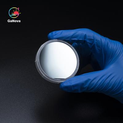
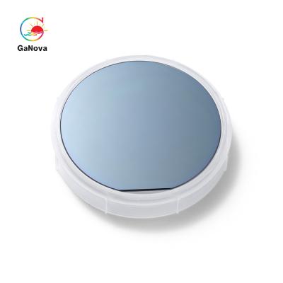
JDCD08-001-007 Γκοφρέτα υποστρώματος C-Plane Sapphire 8 ιντσών
Τιμή: Negotiable
MOQ: Negotiable
Ωρα παράδοσης: Negotiable
Υψηλό Φως:8inch Sapphire Substrate Wafer
JDCD08-001-007 Γκοφρέτα υποστρώματος 6 ιντσών C-Plane Sapphire
Το ρουμπίνι και τα ζαφείρια είναι και τα δύο κατασκευασμένα από κορούνδιο (οξείδιο αλουμινίου - Al2O3).Το κορούνδιο είναι μια από τις πιο σκληρές γνωστές φυσικές ουσίες μετά το διαμάντι.Επιπλέον, επειδή το κορούνδιο είναι τόσο σκληρό και... Δείτε περισσότερα
➤ Επίσκεψη Δικτυακός τόπος
4 ιντσών N-Type UID-Doped GaN On Sapphire Wafer SSP Resistivity>0,5 Ω cm LED, Laser, Επιταξιακή γκοφρέτα PIN
Τιμή: Negotiable
MOQ: Negotiable
Ωρα παράδοσης: 3-4 week days
Μάρκα: GaNova
Υψηλό Φως:PIN GaN On Sapphire Wafer, 4 Inch GaN On Sapphire Wafer
4 ιντσών τύπου N UID-doped GaN σε γκοφρέτα ζαφείρι SSP ειδική αντίσταση>0,5 Ω cm LED, λέιζερ, επιταξιακή γκοφρέτα PIN
Για παράδειγμα, το GaN είναι το υπόστρωμα που καθιστά δυνατές τις ιώδες (405 nm) διόδους λέιζερ, χωρίς τη χρήση μη γραμμικού οπτικού διπλασιασμού συχνότητας.Η ευαισθησία του στην... Δείτε περισσότερα
➤ Επίσκεψη Δικτυακός τόπος

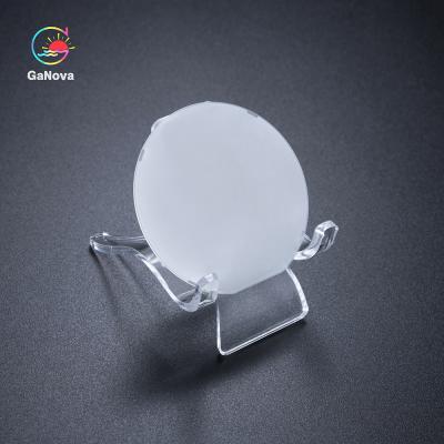
JDCD05-001-004 3*3mm2*0,5mm Electronic Grade Single Crystal Diamond,N Content
Τιμή: Negotiable
MOQ: Negotiable
Ωρα παράδοσης: 3-4 week days
Μάρκα: GaNova
Υψηλό Φως:3*3mm2*0.5mm Single Crystal Diamond
JDCD05-001-004 3*3mm2*0,5mm ηλεκτρονικής ποιότητας μονοκρύσταλλο διαμάντι, περιεκτικότητα N<100ppb, XRD<0,015º Θερμική αγωγιμότητα 1000-2200 για ψύκτρα
ΣΦΑΙΡΙΚΗ ΕΙΚΟΝΑ
Τα διαμάντια CVD είναι πραγματικά διαμάντια.Αν και καλλιεργούνται σε εργαστήριο, τα διαμάντια CVD είναι διαμάντια ποιότητ... Δείτε περισσότερα
➤ Επίσκεψη Δικτυακός τόπος

JDWY01-001-007 Μεμβράνη πάχους 2 ιντσών (4,5 Um AIN σε γκοφρέτα Sapphire, SSP, XRD FWHM Of(002)≤160rcsec\(102) ≤400rcsec
Τιμή: Negotiable
MOQ: Negotiable
Ωρα παράδοσης: Negotiable
Μάρκα: GaNova
Υψηλό Φως:SSP AIN On Sapphire Wafer
Μεμβράνη πάχους 2 ιντσών (4,5) um AIN σε γκοφρέτα ζαφείρι, SSP, XRD FWHM (002)≤160arcsec(102) ≤400rcsec UV απολύμανση, τσιπ LED
Το ζαφείρι είναι ένα υλικό μοναδικού συνδυασμού φυσικών, χημικών και οπτικών ιδιοτήτων, που το καθιστούν ανθεκτικό σε υψηλές θερμοκρασίες, θερμικούς κραδασμούς, διάβρωσ... Δείτε περισσότερα
➤ Επίσκεψη Δικτυακός τόπος